 Hennning
Chiplets
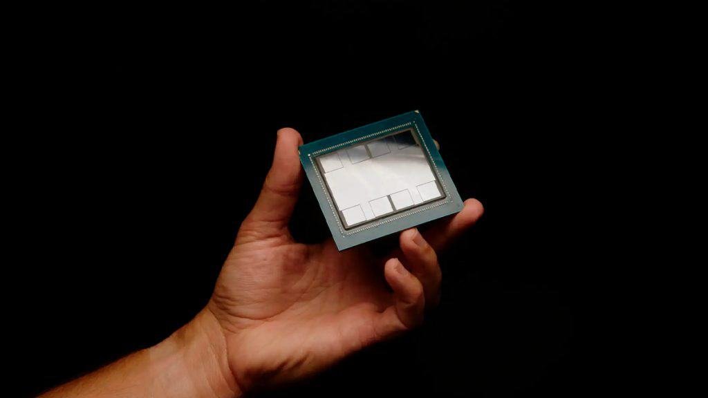
The concept, called chiplets in English, has gained significant traction, with AMD, Apple, Amazon, Tesla, IBM, and Intel showcasing their products. They are rapidly gaining momentum because the chips are cheaper to manufacture, while their packages can surpass the perfection of any slice of silicon.
The strategy, based on advanced packaging technology, has become a key tool for progress in the semiconductor field. It represents one of the biggest changes in recent years for an industry that drives innovation in areas such as AI (artificial intelligence), autonomous vehicles, and military equipment.
“Packaging is where the action happens,” said Subramanian Iyer, a professor of electrical and computer engineering at the University of California, Los Angeles, who helped develop the chip concept. “It’s happening because it’s not true,” he added.
The problem is that this type of packaging, just like chip production, is primarily dominated by companies in Asia. While the U.S. accounts for about 12% of global semiconductor production, U.S. companies provide only 3% of chip packages, according to the IPC trade association.
U.S. industrial policy
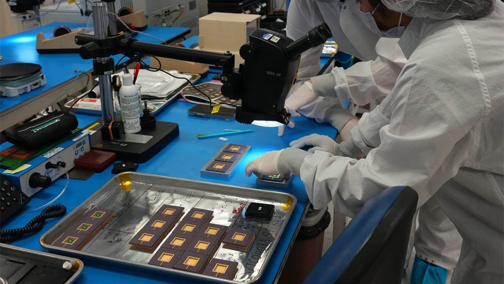
This issue has placed “chiplets” at the center of EU industrial policy formulation. And the CHIPS Act – $52 billion in subsidies (about R$ 260 billion, real value) approved in 2022 – pays for President Biden’s push for domestic processors.
This is because this package will provide money to build more sophisticated factories. Most of it consists of funding advanced packaging factories in the country, to capture more of this essential process.
As smaller chips become, the way you organize chips, which is packaging, becomes increasingly important. And we need this to be done in the U.S.
Gina Raimondo, U.S. Secretary of Commerce, speaking at Georgetown University in February 2023
The Department of Commerce is currently accepting applications for production subsidies through the CHIPS Act. This includes funding for chip packaging factories. It also allocates resources for research programs specifically aimed at advanced packaging.
Some chip packaging companies are racing to secure funding. We have Integra Technologies, Wichita, in Kansas. The company announced plans for an $1.8 billion (R$ 9 billion) expansion. But it said that this depends on receiving federal bonds.
Amkor Technology, a packaging service based in Arizona that has most of its operations in Asia, also stated that it has spoken with customers and government officials about manufacturing in the EU.
How chiplets are made
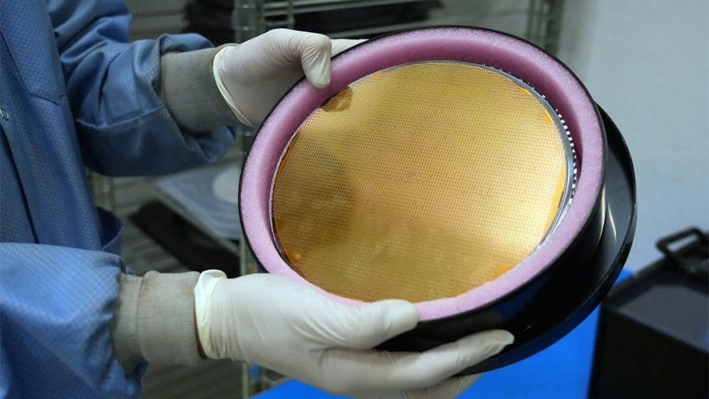
Packaging chips together is not a new concept. Chiplets are just the latest iteration of this idea. It uses technological advancements that help assemble the chips – side by side or stacked on top of each other – along with faster electrical connections between them.
What’s unique about chiplets is the way they are electrically connected.Richard Otte, CEO of Promex Industries, a chip packaging service in Santa Clara, California
Processors cannot connect them to other components. This means they must be placed in some kind of packaging capable of transmitting electrical signals.
This process begins after the factories complete the initial production phase, which is capable of creating hundreds of chips on silicon wafers. Once the wafer is cut, the individual wafers are usually connected to a layer called a substrate, which conducts electrical signals.
The combination is then coated with a protective plastic, creating a package that can be attached to the printed circuit board – essential for connecting with other system components.
Trajectory for processors
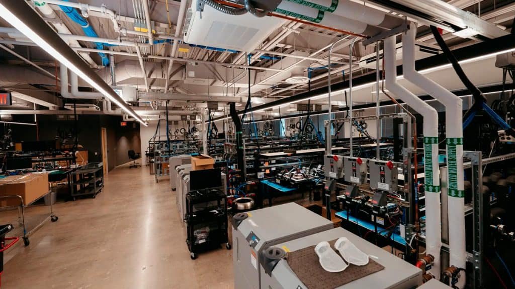
These processes originally required a lot of manual labor, leading Silicon Valley companies to transfer packaging to lower-cost countries in Asia over 50 years ago. Most chips are typically sent to packaging services in countries like Taiwan, Malaysia, South Korea, and China.
Since then, the progress of our packaging has gained importance, due to the diminishing returns of Moore’s Law – the acronym for miniaturized chips, after decades of impulsive progress in Silicon Valley. Its name comes from Gordon Moore, co-founder of Intel, whose 1965 paper described the speed at which companies doubled the number of transistors in a typical processor, improving the performance of a small client.
Today, however, smaller transistors are not necessarily cheaper. In part because building chip factories can cost between $10 billion (R$ 50 billion) and $20 billion (R$ 100 billion).
Large and complex processors are also expensive to design and tend to have more manufacturing defects. Even when companies in areas like generative AI (the technology for ChatGPT, for example) want more transistors than we can currently fit into our leading chips that enable machine production.
Naturally, this is about putting more things in a package.Anirudh Devgan, CEO of Cadence Design Systems
Devgan’s software is used to design conventional processors and chiplet products.
One competitor, Synopsys, said it has tracked over 140 customer designs based on multiprocessor packaging. According to Yole Group, a market research firm, 80% of microprocessors will use chip-style designs by 2027.
Current Situation
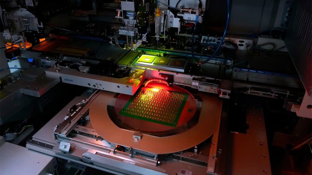
Today, companies generally design the axis of “chiplets” in a package along with their own connection technology. Most industry groups are working on technical standards to make it easier for companies to assemble chip products from different manufacturers.
The new technology is now primarily used for extreme performances. Intel recently launched a processor called Ponte Vecchio with 47 chips that will be used in a powerful supercomputer at Argonne National Laboratory, located near Chicago.
In January, AMD revealed plans for a low-cost product: the MI300. It combines chips for standard calculations with others designed for graphics along with a large set of memory chips.
Aimed at powering another advanced supercomputer at Lawrence Livermore National Laboratory, the processor features 146 billion transistors, compared to tens of billions in the most advanced conventional chips.
Financial Return from Chiplets
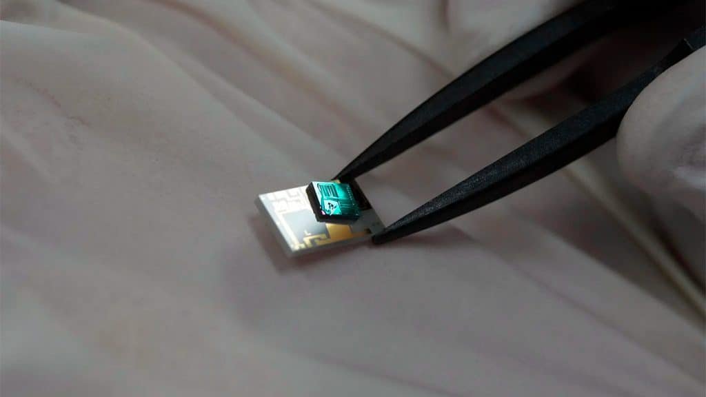
Chiplets have been valuable and foam for AMD. The company is selling over 12 million chips based on the 2017 idea, according to an agreement with Mercury Research. It has become a major player in the field of microprocessors that power the web.
Packaging and crisis services for external devices provide substrates for processors that are in crisis to connect to circuits and other externals. They express significant boosts to the chip boom and to Taiwan Semiconductor Manufacturing Company. The company already manufactures chips for AMD and hundreds of others, in addition to providing an advanced silicon-based substrate called interposer.
Intel is developing similar technology because, by enhancing conventional plastic inputs, it is cheaper in a preferred approach. Among them is Eliyan, a Silicon Valley startup. Intel is also working on new packaging prototypes as part of the Pentagon’s program. And it hopes to gain support from the CHIPS Act for new packaging manufacturing.
Substrate Issue
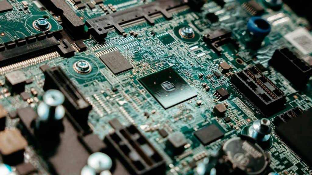
The U.S. does not have major manufacturers of these substrates, which are primarily produced in Asia and evolved from technologies used in circuit board production. Many U.S. companies have also left this business, while they are concerned that industry groups hope to stimulate federal funding. This would help cardboard suppliers start manufacturing substrates.
In March, Biden identified advanced packaging and domestic printed circuit board production as essential for national security. The president also announced $50 million (R$ 250 million) in Defense Production Act funding for companies in the United States and Canada.
Even with these subsidies, gathering the necessary elements to reduce the EU’s dependence on Asian companies is “a major challenge,” said Andreas Olofsson, who led Defense Department research in the area before founding a packaging startup called Zero ASIC.
You are not a supplier. You do not have a workforce. You do not have the equipment. You have to start from scratch.